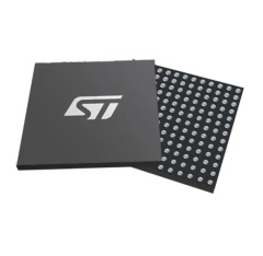
• STM32H7B3AII6Q
  • STM32H7B3AII6Q

STM32H7B3AII6Q

High-performance and DSP with DP-FPU, Arm Cortex-M7 MCU with 2MBytes of Flash memory, 1376 KB SRAM, 280 MHz CPU, L1 cache, graphic accelerations, external memory interfaces, SMPS and large set of peripherals
Supply Voltage Min Volt 1.62
Supply Voltage Max Volt 3.6
Operating Temp Min Celsius -40.0
Operating Temp Max Celsius 85.0
Core Arm Cortex-M7
ECCN US 5A992.c
ECCN EU NEC
Packing Type Tray
RoHs compliant Ecopack2
Grade Industrial
Package Name UFBGA 169 7x7x0.6 P 0.5 mm
Description

STM32H7B3xI devices are based on the high-performance Arm® Cortex®-M7 32-bit RISC core operating at up to 280 MHz. The Cortex® -M7 core features a floating point unit (FPU) which supports Arm® double-precision (IEEE 754 compliant) and single-precision data-processing instructions and data types. STM32H7B3xI devices support a full set of DSP instructions and a memory protection unit (MPU) to enhance application security.

STM32H7B3xI devices incorporate high-speed embedded memories with a dual-bank Flash memory of 2 Mbytes, around 1.4 Mbyte of RAM (including 192 Kbytes of TCM RAM, 1.18 Mbytes of user SRAM and 4 Kbytes of backup SRAM), as well as an extensive range of enhanced I/Os and peripherals connected to four APB buses, three AHB buses, a 32-bit multi-AHB bus matrix and a multi layer AXI interconnect supporting internal and external memory access.

All the devices offer two ADCs, two DACs (one dual and one single DAC), two ultra-low power comparators, a low-power RTC, 12 general-purpose 16-bit timers, two PWM timers for motor control, three low-power timers, a true random number generator (RNG), and a cryptographic acceleration cell and a HASH processor. The devices support nine digital filters for external sigma delta modulators (DFSDM). They also feature standard and advanced communication interfaces.

Key features
  • Core
    • 32-bit Arm® Cortex®-M7 core with double-precision FPU and L1 cache: 16 Kbytes of data and 16 Kbytes of instruction cache allowing to fill one cache line in a single access from the 128-bit embedded Flash memory; frequency up to 280 MHz, MPU, 599 DMIPS/ 2.14 DMIPS/MHz (Dhrystone 2.1), and DSP instructions
  • Memories
    • 2 Mbytes of Flash memory with read while write support, plus 1 Kbyte of OTP
    • ~1.4 Mbytes of RAM: 192 Kbytes of TCM RAM (inc. 64 Kbytes of ITCM RAM + 128 Kbytes of DTCM RAM for time critical routines), 1.18 Mbytes of user SRAM, and 4 Kbytes of SRAM in Backup domain
    • 2x Octo-SPI memory interfaces with on-the-fly
      decryption, I/O multiplexing and support for serial PSRAM/NOR, Hyper RAM/Flash frame formats, running up to 140 MHz in SRD mode and up to 110 MHz in DTR mode
    • Flexible external memory controller with up to 32-bit data bus:
        • SRAM, PSRAM, NOR Flash memory clocked up to 125 MHz in Synchronous mode

        • SDRAM/LPSDR SDRAM,

      • 8/16-bit NAND Flash memory
    • CRC calculation unit
  • Security
    • ROP, PC-ROP, active tamper, secure firmware upgrade support, Secure access mode
  • General-purpose input/outputs
    • Up to 168 I/O ports with interrupt capability
        • Fast I/Os capable of up to 133 MHz

      • Up to 164 5 V-tolerant I/Os
  • Low-power consumption
    • Stop: down to 32 µA with full RAM retention
    • Standby: 2.8 µA (Backup SRAM OFF, RTC/LSE ON, PDR OFF)
    • VBAT: 0.8 µA with RTC and LSE ON
  • Clock management
    • Internal oscillators: 64 MHz HSI, 48 MHz RC, 4 MHz CSI, 32 kHz LSI
    • External oscillators: 4-50 MHz HSE, 32.768 kHz LSE
  • STM32H7B3AII6Q

Download